Journals > > Topics > Integrated Optics
Integrated Optics|188 Article(s)
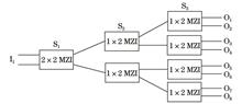
1×8 Silicon-Based Thermo-Optic Switch Based on Mach-Zehnder Interferometers
Xiaoyong Gao, Yangyang Liu, Guangxi Hu, Liangjun Lu, and Haimei Luo
ObjectiveIn recent years, the research on silicon-based thermo-optic (TO) devices has focused on in-depth direction and become more complex, and the realization of higher-performance silicon-based TO devices is the main purpose of our research. There are many kinds of silicon-based optical switches developed so far. We design Mach-Zehnder interferometer (MZI)-type silicon-based TO switches with large bandwidth, simple structure, and high robustness, and the N×N TO-integrated switches and the electro-optic (EO)-integrated switches have been widely studied. The EO switch has a fast switching speed (nanosecond level), but its crosstalk and insertion loss are high due to the free carrier absorption effect. In contrast, TO switches excel in maintaining low loss and low crosstalk, but their switching response time is intrinsically limited, typically on the microsecond scale. Optical switches in hybrid network systems are typically used to handle high-capacity and high-bandwidth optical communication services, making TO switches the preferred choice due to their low loss and low crosstalk characteristics.MethodsThe MZI-type 1×8 silicon-based TO switch proposed and prepared in this paper is composed of one 2×2 MZI and six 1×2 MZI switching units connected by a binary tree structure, which has two input ports and eight output ports in the optical switch, with the first stage comprising a 2×2 MZI switching unit, the second stage comprising two 1×2 MZI switching units, and the third stage comprising four 1×2 MZI switching units. Effective control of the optical signals is achieved by the phase shift of the TO-tuned phase shifter, which directs the light to the destination branch waveguide, thus realizing the optical switching function. The coupler and phase shifter in the optical switching unit are optimized by using the finite-difference time-domain method and the particle swarm optimization algorithm to improve the switching performance and reduce the chip size. The long connecting waveguide is designed as a wide waveguide of 2 to reduce the waveguide transmission loss. The package connects the optical switch chip to a 14-channel optical fiber array by using an end-face coupling, curing it with an ultraviolet curing adhesive. In addition, a multi-channel voltage source is designed, which mainly consists of a CPU, op-amp LM324, analogue switches, and four DAC modules. This multi-channel voltage source has 32 selective ports, and the synchronous switching of the optical switching ports is achieved by simultaneously regulating the voltages of all levels of thermal phase shifters through the host computer. The results show that the optical switch achieves low on-chip insertion loss, lower crosstalk, and a reduced response time of the optical switch.Results and DiscussionsThe experiments demonstrate that the designed and prepared 1×8 TO switch performs well in all aspects; its average on-chip insertion loss is about 1.1 dB (Fig. 8); the fiber-to-fiber loss fluctuates and varies in different paths because the difference in connecting waveguide lengths of the different paths and different ports with different coupling efficiencies to the fiber may not be the same. The crosstalk of its eight output ports is less than -23.6 dB (Fig. 9), and the crosstalk is the leading cause of switching signal degradation. The 2×2 MMI coupler can reduce crosstalk. The response time of the switch is less than 60 μs (Fig. 11) because the thickness of the silica cladding layer at the bottom is more significant than that of the buffer layer. The thermal conductivity of silica is about 1/100 of that of silicon; after heating, the heat diffusion from the core layer to the substrate is slower, and the falling-edge time is longer than that of the rising-edge time. When the input electrical signal's frequency is high, the TO phase shifter's response can no longer follow the electrical signal due to its limited response bandwidth, and the response is no longer square-wave in character. However, the rise and fall time becomes shorter. In addition, there is a difference in the response time of the switch due to manufacturing process errors in different phase shifters.ConclusionsOur proposed 1×8 optical switch chip is based on a tree structure consisting of one 2×2 MZI and six 1×2 MZIs, with a TiN heater in each thermal phase shifter's upper/lower arm. The switch chip is constructed on a SOI platform by using a CMOS-compatible process with a size of 1.75 mm×3 mm. The chip exhibits an on-chip insertion loss of about 1.1 dB at the operating wavelength of 1550 nm, a crosstalk of less than -23.6 dB, a response time of the switch of better than 60 μs, and an average power dissipation of the switch of about 34.09 mW. The experimental results show that the 1×8 TO switch has the advantages of compactness, low loss, and low crosstalk. ObjectiveIn recent years, the research on silicon-based thermo-optic (TO) devices has focused on in-depth direction and become more complex, and the realization of higher-performance silicon-based TO devices is the main purpose of our research. There are many kinds of silicon-based optical switches developed so far. We design Mach-Zehnder interferometer (MZI)-type silicon-based TO switches with large bandwidth, simple structure, and high robustness, and the N×N TO-integrated switches and the electro-optic (EO)-integrated switches have been widely studied. The EO switch has a fast switching speed (nanosecond level), but its crosstalk and insertion loss are high due to the free carrier absorption effect. In contrast, TO switches excel in maintaining low loss and low crosstalk, but their switching response time is intrinsically limited, typically on the microsecond scale. Optical switches in hybrid network systems are typically used to handle high-capacity and high-bandwidth optical communication services, making TO switches the preferred choice due to their low loss and low crosstalk characteristics.MethodsThe MZI-type 1×8 silicon-based TO switch proposed and prepared in this paper is composed of one 2×2 MZI and six 1×2 MZI switching units connected by a binary tree structure, which has two input ports and eight output ports in the optical switch, with the first stage comprising a 2×2 MZI switching unit, the second stage comprising two 1×2 MZI switching units, and the third stage comprising four 1×2 MZI switching units. Effective control of the optical signals is achieved by the phase shift of the TO-tuned phase shifter, which directs the light to the destination branch waveguide, thus realizing the optical switching function. The coupler and phase shifter in the optical switching unit are optimized by using the finite-difference time-domain method and the particle swarm optimization algorithm to improve the switching performance and reduce the chip size. The long connecting waveguide is designed as a wide waveguide of 2 to reduce the waveguide transmission loss. The package connects the optical switch chip to a 14-channel optical fiber array by using an end-face coupling, curing it with an ultraviolet curing adhesive. In addition, a multi-channel voltage source is designed, which mainly consists of a CPU, op-amp LM324, analogue switches, and four DAC modules. This multi-channel voltage source has 32 selective ports, and the synchronous switching of the optical switching ports is achieved by simultaneously regulating the voltages of all levels of thermal phase shifters through the host computer. The results show that the optical switch achieves low on-chip insertion loss, lower crosstalk, and a reduced response time of the optical switch.Results and DiscussionsThe experiments demonstrate that the designed and prepared 1×8 TO switch performs well in all aspects; its average on-chip insertion loss is about 1.1 dB (Fig. 8); the fiber-to-fiber loss fluctuates and varies in different paths because the difference in connecting waveguide lengths of the different paths and different ports with different coupling efficiencies to the fiber may not be the same. The crosstalk of its eight output ports is less than -23.6 dB (Fig. 9), and the crosstalk is the leading cause of switching signal degradation. The 2×2 MMI coupler can reduce crosstalk. The response time of the switch is less than 60 μs (Fig. 11) because the thickness of the silica cladding layer at the bottom is more significant than that of the buffer layer. The thermal conductivity of silica is about 1/100 of that of silicon; after heating, the heat diffusion from the core layer to the substrate is slower, and the falling-edge time is longer than that of the rising-edge time. When the input electrical signal's frequency is high, the TO phase shifter's response can no longer follow the electrical signal due to its limited response bandwidth, and the response is no longer square-wave in character. However, the rise and fall time becomes shorter. In addition, there is a difference in the response time of the switch due to manufacturing process errors in different phase shifters.ConclusionsOur proposed 1×8 optical switch chip is based on a tree structure consisting of one 2×2 MZI and six 1×2 MZIs, with a TiN heater in each thermal phase shifter's upper/lower arm. The switch chip is constructed on a SOI platform by using a CMOS-compatible process with a size of 1.75 mm×3 mm. The chip exhibits an on-chip insertion loss of about 1.1 dB at the operating wavelength of 1550 nm, a crosstalk of less than -23.6 dB, a response time of the switch of better than 60 μs, and an average power dissipation of the switch of about 34.09 mW. The experimental results show that the 1×8 TO switch has the advantages of compactness, low loss, and low crosstalk.
Acta Optica Sinica
- Publication Date: Apr. 25, 2024
- Vol. 44, Issue 8, 0813001 (2024)

Metamaterial Terahertz Band-Stop Filter Based on Two Intersecting Split-Ring Resonance
Hang Yuan, Wangting Fu, Zuyao Liu, Zhiming Rao, Xingfang Luo, Guanhua Zhu, Shuaike Wu, and Wei Chen
ObjectiveTerahertz filter is an important functional device for realizing terahertz imaging, terahertz communication, and other terahertz application technologies, and in-depth study of terahertz filters plays a great role in promoting the development of terahertz technologies. Therefore, the design of terahertz filters with a wide range of adjustable center frequency, sensitive bandwidth adjustment, deep modulation depth, simple structure, and multi-band transmission performance has become an urgent problem. In this study, a metamaterial terahertz band-stop filter based on two intersecting split-ring resonance (TI-SRR) is designed. It can effectively expand the bandwidth adjustment range, adjust the center frequency, reduce the transmittance, and make the stopband attenuate rapidly. At the same time, it has multi-band filtering and is easy to fabricate and process. The metamaterial terahertz band-stop filter has high application value in the field of new communication equipment and precision instruments.MethodsIn this experiment, the effect of each parameter on the performance of the filter is investigated by varying the line width, inter-ring spacing, and radius size of the TI-SRR. The transmission coefficients of the filter under each parameter are compared, and the design scheme with the best performance is summarized. The electric field and surface current distributions at the three resonance points of the metamaterial band-stop filter are analyzed, so as to investigate the working mechanism of the filter. In order to verify the calculation results of the theoretical model, physical samples of the filter are prepared by micro-nanolithography and tested using a terahertz time-domain spectroscopy (THz-TDS) system. The results of the actual measurement and simulation are compared to find the cause of the error.Results and DiscussionsSimulation experiments are carried out on several parameters of the metamaterial terahertz band-stop filter, while other parameters are kept unchanged. When the line width w gradually increases from 2 to 14 µm, the filter's first stopband bandwidth increases from 0.190 to 0.253 THz, and the relative bandwidth radually increases from 44.98% to 54.33%. The bandwidth range increases, and the center frequency is shifted to the high-frequency direction, while the filter's modulation depth deepens. However, as the line width increases, the resonance in the ring is strong, and clutter appears at high frequencies. The line width w is selected to be 10 µm (Fig. 2). When the spacing m gradually increases from 10 to 40 µm, the first stopband bandwidth of the filter decreases from 0.238 to 0.227 THz, and the relative bandwidth gradually decreases from 52.44% to 44.51%. The bandwidth of the filter decreases slightly, and the adjustment of the spacing allows the filter bandwidth to be adjusted precisely. The transmittance of the filter is gradually increasing, which is not favorable to the performance of the band-stop filter. Therefore, smaller spacing indicates a better filtering effect. However, as the spacing m decreases, the resonance in the ring becomes stronger, and clutter occurs at high frequencies. The spacing m is selected to be 10 µm (Fig. 3). When the outer radius R1 gradually increases from 56 to 68 µm, the inner radius R2 gradually increases from 56 to 58 µm, and the first stopband bandwidth of the filter increases from 0.222 to 0.261 THz. The relative bandwidth increases from 47.65% to 61.34%, and the effective bandwidth of the filter increases. The filter performance transmittance is reduced within the effective bandwidth, and the filter performance is improved. However, with the gradual increase in the radius, the filtering effect of the third resonance point becomes worse, and the outer radius R1 is selected to be 60 µm after comprehensive consideration (Fig. 4). The physical samples of the filter are prepared by micro-nano lithography (Fig. 10). The measured results are shifted at each resonance point compared with the simulation, and the measured stop-band suppression effect is not as good as that of the simulation. Especially, the gap is obvious at the high frequency, but the overall curve trend remains consistent.ConclusionsIn this study, a terahertz band-stop filter based on metamaterials is designed to optimize the performance of the filter by varying the metal line width, inter-ring spacing, and metal open-ring radius, and the optimal design is concluded. The working mechanism of the filter is analyzed based on the electric field and surface current distributions of the terahertz filter. The physical filter samples are prepared by micro-nano lithography and tested by the THz-TDS system. Test results are comparable with the simulation results considering the errors in the test process. The band-stop filter has the advantages of a simple structure, adjustable center frequency, fine-tunable bandwidth, wide range adjustment, low stopband transmittance, and deep modulation depth. ObjectiveTerahertz filter is an important functional device for realizing terahertz imaging, terahertz communication, and other terahertz application technologies, and in-depth study of terahertz filters plays a great role in promoting the development of terahertz technologies. Therefore, the design of terahertz filters with a wide range of adjustable center frequency, sensitive bandwidth adjustment, deep modulation depth, simple structure, and multi-band transmission performance has become an urgent problem. In this study, a metamaterial terahertz band-stop filter based on two intersecting split-ring resonance (TI-SRR) is designed. It can effectively expand the bandwidth adjustment range, adjust the center frequency, reduce the transmittance, and make the stopband attenuate rapidly. At the same time, it has multi-band filtering and is easy to fabricate and process. The metamaterial terahertz band-stop filter has high application value in the field of new communication equipment and precision instruments.MethodsIn this experiment, the effect of each parameter on the performance of the filter is investigated by varying the line width, inter-ring spacing, and radius size of the TI-SRR. The transmission coefficients of the filter under each parameter are compared, and the design scheme with the best performance is summarized. The electric field and surface current distributions at the three resonance points of the metamaterial band-stop filter are analyzed, so as to investigate the working mechanism of the filter. In order to verify the calculation results of the theoretical model, physical samples of the filter are prepared by micro-nanolithography and tested using a terahertz time-domain spectroscopy (THz-TDS) system. The results of the actual measurement and simulation are compared to find the cause of the error.Results and DiscussionsSimulation experiments are carried out on several parameters of the metamaterial terahertz band-stop filter, while other parameters are kept unchanged. When the line width w gradually increases from 2 to 14 µm, the filter's first stopband bandwidth increases from 0.190 to 0.253 THz, and the relative bandwidth radually increases from 44.98% to 54.33%. The bandwidth range increases, and the center frequency is shifted to the high-frequency direction, while the filter's modulation depth deepens. However, as the line width increases, the resonance in the ring is strong, and clutter appears at high frequencies. The line width w is selected to be 10 µm (Fig. 2). When the spacing m gradually increases from 10 to 40 µm, the first stopband bandwidth of the filter decreases from 0.238 to 0.227 THz, and the relative bandwidth gradually decreases from 52.44% to 44.51%. The bandwidth of the filter decreases slightly, and the adjustment of the spacing allows the filter bandwidth to be adjusted precisely. The transmittance of the filter is gradually increasing, which is not favorable to the performance of the band-stop filter. Therefore, smaller spacing indicates a better filtering effect. However, as the spacing m decreases, the resonance in the ring becomes stronger, and clutter occurs at high frequencies. The spacing m is selected to be 10 µm (Fig. 3). When the outer radius R1 gradually increases from 56 to 68 µm, the inner radius R2 gradually increases from 56 to 58 µm, and the first stopband bandwidth of the filter increases from 0.222 to 0.261 THz. The relative bandwidth increases from 47.65% to 61.34%, and the effective bandwidth of the filter increases. The filter performance transmittance is reduced within the effective bandwidth, and the filter performance is improved. However, with the gradual increase in the radius, the filtering effect of the third resonance point becomes worse, and the outer radius R1 is selected to be 60 µm after comprehensive consideration (Fig. 4). The physical samples of the filter are prepared by micro-nano lithography (Fig. 10). The measured results are shifted at each resonance point compared with the simulation, and the measured stop-band suppression effect is not as good as that of the simulation. Especially, the gap is obvious at the high frequency, but the overall curve trend remains consistent.ConclusionsIn this study, a terahertz band-stop filter based on metamaterials is designed to optimize the performance of the filter by varying the metal line width, inter-ring spacing, and metal open-ring radius, and the optimal design is concluded. The working mechanism of the filter is analyzed based on the electric field and surface current distributions of the terahertz filter. The physical filter samples are prepared by micro-nano lithography and tested by the THz-TDS system. Test results are comparable with the simulation results considering the errors in the test process. The band-stop filter has the advantages of a simple structure, adjustable center frequency, fine-tunable bandwidth, wide range adjustment, low stopband transmittance, and deep modulation depth.
Acta Optica Sinica
- Publication Date: Mar. 10, 2024
- Vol. 44, Issue 5, 0513001 (2024)

Adjustment Method and Strain Sensing Characteristics of Whispering Gallery Mode Resonance in Hollow Microbottle
Lu Cai, Shangwen Li, Jin Wang, Jun Liu, Fucheng Xiang, and Zhongjia Li
ObjectiveThe whispering gallery mode resonator (WGMR) has a very high quality factor and a very small mode volume, so it has great advantages in the fields of laser, optical communication, and biomedical detection. Because different applications may have different requirements for resonance peak parameters, scholars have proposed a series of resonance peak tuning methods. The tuning parameters include the wavelength of the resonance peak, Q value, coupling efficiency, etc. The resonant wavelength is directly related to the refractive index and size of the resonant cavity. In addition, the mechanical tuning method is the most simple and feasible method to control the WGM resonant wavelength in a wide range. In this paper, a double-handle hollow microbottle is proposed to achieve a simple and feasible wide-range tuning of WGM. The double-handle hollow microbottle is fabricated by using single-mode fiber, and the excited whispering gallery mode propagates in the thin wall of the hollow microbottle. By controlling the axial tensile strain, the diameter of the microcavity and the thickness of the microcavity wall can be adjusted, thereby realizing the tuning of the resonant wavelength and the quality factor Q of the whispering gallery mode.MethodsFirst, the influence of controlling the temperature and stress on the resonant peak wavelength is analyzed theoretically. For the selected l-order WGM, if the environment temperature is changed, the relative variation of the resonant wavelength is determined by the effective refractive index and the microcavity radius. The stress regulation method is to apply an external force to the resonant cavity to deform the cavity, and the refractive index of the microcavity is affected by the photoelastic effect. The quality factor Q is related to the light field energy stored in the resonant cavity and the loss energy per cycle. When the microcavity is stretched, it will affect the radiation loss and coupling loss, thereby regulating the Q value. Second, in terms of the preparation of the structure, two sections of flat Er-doped fiber are vertically inserted into the etching solution for corrosion. Then, the two sections of Er-doped fiber after corrosion are placed on the motors on both sides of the fiber fusion splicer, and the two sections of Er-doped fiber with the concave surface are spliced together by arc discharge to obtain a hollow microbottle. On the basis of the hollow microbottle, the asymmetric hollow microbottle is obtained by using the welding machine to pull the cone on the side of the microcavity. Third, the tapered fiber is fixed, and the microcavity is constrained to be perpendicular to the tapered fiber. The two three-dimensional displacement stages hold the fiber at both ends of the microbottle cavity, which can accurately adjust the coupling distance between the tapered fiber and the microbottle cavity and can control the stretching amount of the fiber at both ends of the micro-cavity, thereby applying axial stress. The whole coupling process is completed with the assistance of a high-definition electron microscope, which is used to observe the coupling state of the composite microcavity and the tapered fiber. The tuning results are observed by spectral changes.Results and DiscussionsUnder the action of strain, the axial elongation of the hollow microbottle leads to a decrease in the radius and refractive index of the resonant cavity, which makes the resonant peak move to the short wavelength, and it is consistent with the description of the resonant wavelength change in Eq. (3). Figure 4(b) gives the relationship curve between the resonance peak and the strain change. The wavelength tuning efficiency of the resonance peak is 0.482 pm/με; the wavelength tuning range of the resonance peak is 0.4 nm, and the linearity can reach 0.999. By applying strain to the resonant cavity, the wavelength corresponding to a certain resonant mode can be adjusted to the expected value. It can be seen from Fig. 5 that when the strain applied to the microbottle is gradually increased, the Q value of the resonance peak at 1548.92 nm increases first and then decreases during the process of moving to 1548.83 nm. According to the analysis in 2.2 section, it can be seen that this is related to the change of coupling loss. The tuning range of the asymmetric hollow microbottle cavity structure is increased to 0.66 nm (Fig. 7). We put the tuning sensitivity of the two structures into a figure for comparison, as shown in Fig. 7(b). By means of asymmetric tapering, the tuning sensitivity of the external strain to the WGM resonance peak increases to 0.795 pm/με, and the linearity reaches 0.999. If it is used as a strain sensor, the Q value of the resonance peak can reach 7.218×10⁴, and the strain sensing resolution can reach 25 με.ConclusionsIn this paper, a quartz fiber double-handle hollow microbottle prepared by the etching-fusion method is designed. The refractive index and diameter of the microcavity are changed by the axial stretching method, so as to tune the resonant wavelength and quality factor Q of whispering gallery mode. The tuning efficiency is 0.482 pm/με, and the tuning range is 0.4 nm. On this basis, the microcavity structure is improved by asymmetric tapering so that the physical parameters of the microcavity are more sensitive to axial strain. The tuning range of the resonant wavelength reaches 0.66 nm, and the tuning efficiency is increased to 0.795 pm/με. At the same time, the whispering gallery mode tuning method proves that the microcavity has strain sensing ability; the resolution is less than 25 με, and the linearity is 0.999, which provides a new idea for high-resolution strain sensing. ObjectiveThe whispering gallery mode resonator (WGMR) has a very high quality factor and a very small mode volume, so it has great advantages in the fields of laser, optical communication, and biomedical detection. Because different applications may have different requirements for resonance peak parameters, scholars have proposed a series of resonance peak tuning methods. The tuning parameters include the wavelength of the resonance peak, Q value, coupling efficiency, etc. The resonant wavelength is directly related to the refractive index and size of the resonant cavity. In addition, the mechanical tuning method is the most simple and feasible method to control the WGM resonant wavelength in a wide range. In this paper, a double-handle hollow microbottle is proposed to achieve a simple and feasible wide-range tuning of WGM. The double-handle hollow microbottle is fabricated by using single-mode fiber, and the excited whispering gallery mode propagates in the thin wall of the hollow microbottle. By controlling the axial tensile strain, the diameter of the microcavity and the thickness of the microcavity wall can be adjusted, thereby realizing the tuning of the resonant wavelength and the quality factor Q of the whispering gallery mode.MethodsFirst, the influence of controlling the temperature and stress on the resonant peak wavelength is analyzed theoretically. For the selected l-order WGM, if the environment temperature is changed, the relative variation of the resonant wavelength is determined by the effective refractive index and the microcavity radius. The stress regulation method is to apply an external force to the resonant cavity to deform the cavity, and the refractive index of the microcavity is affected by the photoelastic effect. The quality factor Q is related to the light field energy stored in the resonant cavity and the loss energy per cycle. When the microcavity is stretched, it will affect the radiation loss and coupling loss, thereby regulating the Q value. Second, in terms of the preparation of the structure, two sections of flat Er-doped fiber are vertically inserted into the etching solution for corrosion. Then, the two sections of Er-doped fiber after corrosion are placed on the motors on both sides of the fiber fusion splicer, and the two sections of Er-doped fiber with the concave surface are spliced together by arc discharge to obtain a hollow microbottle. On the basis of the hollow microbottle, the asymmetric hollow microbottle is obtained by using the welding machine to pull the cone on the side of the microcavity. Third, the tapered fiber is fixed, and the microcavity is constrained to be perpendicular to the tapered fiber. The two three-dimensional displacement stages hold the fiber at both ends of the microbottle cavity, which can accurately adjust the coupling distance between the tapered fiber and the microbottle cavity and can control the stretching amount of the fiber at both ends of the micro-cavity, thereby applying axial stress. The whole coupling process is completed with the assistance of a high-definition electron microscope, which is used to observe the coupling state of the composite microcavity and the tapered fiber. The tuning results are observed by spectral changes.Results and DiscussionsUnder the action of strain, the axial elongation of the hollow microbottle leads to a decrease in the radius and refractive index of the resonant cavity, which makes the resonant peak move to the short wavelength, and it is consistent with the description of the resonant wavelength change in Eq. (3). Figure 4(b) gives the relationship curve between the resonance peak and the strain change. The wavelength tuning efficiency of the resonance peak is 0.482 pm/με; the wavelength tuning range of the resonance peak is 0.4 nm, and the linearity can reach 0.999. By applying strain to the resonant cavity, the wavelength corresponding to a certain resonant mode can be adjusted to the expected value. It can be seen from Fig. 5 that when the strain applied to the microbottle is gradually increased, the Q value of the resonance peak at 1548.92 nm increases first and then decreases during the process of moving to 1548.83 nm. According to the analysis in 2.2 section, it can be seen that this is related to the change of coupling loss. The tuning range of the asymmetric hollow microbottle cavity structure is increased to 0.66 nm (Fig. 7). We put the tuning sensitivity of the two structures into a figure for comparison, as shown in Fig. 7(b). By means of asymmetric tapering, the tuning sensitivity of the external strain to the WGM resonance peak increases to 0.795 pm/με, and the linearity reaches 0.999. If it is used as a strain sensor, the Q value of the resonance peak can reach 7.218×10⁴, and the strain sensing resolution can reach 25 με.ConclusionsIn this paper, a quartz fiber double-handle hollow microbottle prepared by the etching-fusion method is designed. The refractive index and diameter of the microcavity are changed by the axial stretching method, so as to tune the resonant wavelength and quality factor Q of whispering gallery mode. The tuning efficiency is 0.482 pm/με, and the tuning range is 0.4 nm. On this basis, the microcavity structure is improved by asymmetric tapering so that the physical parameters of the microcavity are more sensitive to axial strain. The tuning range of the resonant wavelength reaches 0.66 nm, and the tuning efficiency is increased to 0.795 pm/με. At the same time, the whispering gallery mode tuning method proves that the microcavity has strain sensing ability; the resolution is less than 25 με, and the linearity is 0.999, which provides a new idea for high-resolution strain sensing.
Acta Optica Sinica
- Publication Date: Jan. 25, 2024
- Vol. 44, Issue 2, 0213001 (2024)
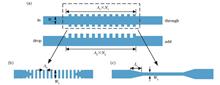
Ultra-High-Bandwidth Silicon-Based Photonic Filter for Coarse Wavelength Division Multiplexing Systems
Shasha Liao, Cong Huang, Yuting Feng, Wuhao Zhang, Shuai Zhao, and Zhenwei Liu
ObjectiveWith the continuous development of scientific and technological information, people's demand for communication system capacity and speed is increasing, and wavelength division multiplexing technology plays an important role in improving system capacity. As a key component of wavelength division multiplexing systems, the demultiplexer has become a research hotspot in this field. At present, a large-bandwidth filter with a high rectangular degree is mainly used to realize the function of demultiplexing. High-bandwidth and ultra-high-bandwidth filter schemes are frequently proposed and implemented, involving photonic crystals, Mach-Zehnder interferometers, and waveguide Bragg gratings. Although traditional schemes based on photonic crystals and waveguide Bragg gratings can achieve large bandwidths, additional magneto-optical devices such as optical circulators need to be added to separate the reflected signals due to their working in the reflection mode, which undoubtedly increases the complexity of the system. In addition, the difficulty in the large-scale integration of magneto-optical materials with silicon-based devices also affects the application range of the above schemes. The Mach-Zehnder interferometer scheme is also difficult to integrate on a large scale due to its large structure size. Therefore, to realize a compact ultra-high-bandwidth filter, this paper proposes a filtering scheme based on a grating-assisted contra-directional coupler structure. The filter has the advantages of a high rectangular degree, an ultra-high bandwidth, and a low loss and can meet the needs of demultiplexing in coarse wavelength division multiplexing systems.MethodsTo reduce the use of magneto-optical devices such as optical circulators and improve integration, this paper uses a grating-assisted contra-directional coupler structure to realize the filter function. According to the coupled mode theory, the bandwidth of the contra-directional coupler is inversely proportional to the sum of the effective refractive indices of the two waveguides and proportional to the coupling coefficient. Therefore, it is necessary to reduce the effective refractive indices of the two waveguides and increase the coupling coefficient for enhancing the bandwidth of the filter. This paper first compares the effective refractive indices of sub-wavelength grating and conventional waveguide grating and finds that the former has a lower refractive index. Considering that a smaller waveguide width corresponds to a lower effective refractive index, the paper proposes to gradually change the input waveguide into a narrow waveguide through a taper so that the effective refractive index can be further reduced. When the width of the waveguide is reduced to a certain extent, the effective refractive index is lower than that of the current common scheme. Moreover, the narrow waveguide has a more dispersed electric field, which is beneficial to improve the coupling coefficient and achieve an ultra-high bandwidth. Therefore, in this paper, the narrow waveguide structure and the grating-assisted contra-directional coupler structure are used to address the low bandwidth, and the problem of a large structure size is also solved by continuing to optimize parameters.Results and DiscussionsThe width of the proposed narrow waveguide is 180 nm; the widths of the conventional grating and the sub-wavelength grating are both 500 nm; the duty cycle is 0.5. The effective refractive index of the narrow waveguide in the wavelength range of 1530-1570 nm is 1.441-1.447, which is smaller than those of the conventional grating and the sub-wavelength grating (Fig. 2). To further verify that the filter can achieve higher bandwidth, the transmission matrix method is used to calculate its spectral characteristics. At this time, the 3 dB bandwidth at the drop end is 70 nm (Fig. 3), which is in line with the above theoretical derivation. The grating comb and the waveguide are apodized at the same time to further improve the side-lobe suppression ratio (Fig. 5). In such a case, the 3 dB bandwidth of the filter is 92.9 nm; the side-lobe suppression ratio is greater than 11.1 dB; the shape factor is 0.99; the insertion loss is less than 0.38 dB; the in-band ripple is less than 0.28 dB (Fig. 6). This paper also designs a filtering scheme with a more compact structure and a higher side-lobe suppression ratio. After re-optimization, the 3 dB bandwidth is 87 nm; the side-lobe suppression ratio is 25.6 dB; the device length is 96 μm; the insertion loss is 0.16 dB; the in-band ripple is 0.08 dB (Fig. 7).ConclusionsThis paper proposes an ultra-high-bandwidth filter based on a grating-assisted contra-directional coupler. Firstly, in light of the coupled mode theory, the expression of the filter bandwidth is deduced, and the factors influencing the bandwidth are analyzed. Secondly, the paper develops a method of changing one waveguide in the contra-directional coupler to a narrow waveguide. After design and optimization, an ultra-high-bandwidth silicon-based photonic filter is finally realized with a 3 dB bandwidth of 92.9 nm, a side-lobe suppression ratio of 11.1 dB, a shape factor of 0.99, an insertion loss of 0.38 dB, and an in-band ripple of 0.28 dB. In addition, this paper also designs a filtering scheme with a more compact structure and a higher side-lobe suppression ratio. After re-optimization, the 3 dB bandwidth is 87 nm; the side-lobe suppression ratio is 25.6 dB; the device length is 96 μm; the insertion loss is 0.16 dB; the in-band ripple is 0.08 dB. The two filter schemes proposed in this paper adopt the contra-directional coupling method. The filter bandwidth in scheme 1 is larger than the largest bandwidth of similar structures, and the scheme greatly reduces the size of the filter. Scheme 2 improves the side-lobe suppression ratio and reduces the length of the device, which is suitable for application scenarios that are more sensitive to side-lobe suppression ratio and size. In addition, this paper also focuses on analyzing the filter performance changes when there are process errors in the apodization coefficient and comb width of the grating. A method of increasing the design value of the gap G between the narrow waveguide and the grating and fine-tuning the grating period is proposed to reduce the influence of process errors on filter performance. ObjectiveWith the continuous development of scientific and technological information, people's demand for communication system capacity and speed is increasing, and wavelength division multiplexing technology plays an important role in improving system capacity. As a key component of wavelength division multiplexing systems, the demultiplexer has become a research hotspot in this field. At present, a large-bandwidth filter with a high rectangular degree is mainly used to realize the function of demultiplexing. High-bandwidth and ultra-high-bandwidth filter schemes are frequently proposed and implemented, involving photonic crystals, Mach-Zehnder interferometers, and waveguide Bragg gratings. Although traditional schemes based on photonic crystals and waveguide Bragg gratings can achieve large bandwidths, additional magneto-optical devices such as optical circulators need to be added to separate the reflected signals due to their working in the reflection mode, which undoubtedly increases the complexity of the system. In addition, the difficulty in the large-scale integration of magneto-optical materials with silicon-based devices also affects the application range of the above schemes. The Mach-Zehnder interferometer scheme is also difficult to integrate on a large scale due to its large structure size. Therefore, to realize a compact ultra-high-bandwidth filter, this paper proposes a filtering scheme based on a grating-assisted contra-directional coupler structure. The filter has the advantages of a high rectangular degree, an ultra-high bandwidth, and a low loss and can meet the needs of demultiplexing in coarse wavelength division multiplexing systems.MethodsTo reduce the use of magneto-optical devices such as optical circulators and improve integration, this paper uses a grating-assisted contra-directional coupler structure to realize the filter function. According to the coupled mode theory, the bandwidth of the contra-directional coupler is inversely proportional to the sum of the effective refractive indices of the two waveguides and proportional to the coupling coefficient. Therefore, it is necessary to reduce the effective refractive indices of the two waveguides and increase the coupling coefficient for enhancing the bandwidth of the filter. This paper first compares the effective refractive indices of sub-wavelength grating and conventional waveguide grating and finds that the former has a lower refractive index. Considering that a smaller waveguide width corresponds to a lower effective refractive index, the paper proposes to gradually change the input waveguide into a narrow waveguide through a taper so that the effective refractive index can be further reduced. When the width of the waveguide is reduced to a certain extent, the effective refractive index is lower than that of the current common scheme. Moreover, the narrow waveguide has a more dispersed electric field, which is beneficial to improve the coupling coefficient and achieve an ultra-high bandwidth. Therefore, in this paper, the narrow waveguide structure and the grating-assisted contra-directional coupler structure are used to address the low bandwidth, and the problem of a large structure size is also solved by continuing to optimize parameters.Results and DiscussionsThe width of the proposed narrow waveguide is 180 nm; the widths of the conventional grating and the sub-wavelength grating are both 500 nm; the duty cycle is 0.5. The effective refractive index of the narrow waveguide in the wavelength range of 1530-1570 nm is 1.441-1.447, which is smaller than those of the conventional grating and the sub-wavelength grating (Fig. 2). To further verify that the filter can achieve higher bandwidth, the transmission matrix method is used to calculate its spectral characteristics. At this time, the 3 dB bandwidth at the drop end is 70 nm (Fig. 3), which is in line with the above theoretical derivation. The grating comb and the waveguide are apodized at the same time to further improve the side-lobe suppression ratio (Fig. 5). In such a case, the 3 dB bandwidth of the filter is 92.9 nm; the side-lobe suppression ratio is greater than 11.1 dB; the shape factor is 0.99; the insertion loss is less than 0.38 dB; the in-band ripple is less than 0.28 dB (Fig. 6). This paper also designs a filtering scheme with a more compact structure and a higher side-lobe suppression ratio. After re-optimization, the 3 dB bandwidth is 87 nm; the side-lobe suppression ratio is 25.6 dB; the device length is 96 μm; the insertion loss is 0.16 dB; the in-band ripple is 0.08 dB (Fig. 7).ConclusionsThis paper proposes an ultra-high-bandwidth filter based on a grating-assisted contra-directional coupler. Firstly, in light of the coupled mode theory, the expression of the filter bandwidth is deduced, and the factors influencing the bandwidth are analyzed. Secondly, the paper develops a method of changing one waveguide in the contra-directional coupler to a narrow waveguide. After design and optimization, an ultra-high-bandwidth silicon-based photonic filter is finally realized with a 3 dB bandwidth of 92.9 nm, a side-lobe suppression ratio of 11.1 dB, a shape factor of 0.99, an insertion loss of 0.38 dB, and an in-band ripple of 0.28 dB. In addition, this paper also designs a filtering scheme with a more compact structure and a higher side-lobe suppression ratio. After re-optimization, the 3 dB bandwidth is 87 nm; the side-lobe suppression ratio is 25.6 dB; the device length is 96 μm; the insertion loss is 0.16 dB; the in-band ripple is 0.08 dB. The two filter schemes proposed in this paper adopt the contra-directional coupling method. The filter bandwidth in scheme 1 is larger than the largest bandwidth of similar structures, and the scheme greatly reduces the size of the filter. Scheme 2 improves the side-lobe suppression ratio and reduces the length of the device, which is suitable for application scenarios that are more sensitive to side-lobe suppression ratio and size. In addition, this paper also focuses on analyzing the filter performance changes when there are process errors in the apodization coefficient and comb width of the grating. A method of increasing the design value of the gap G between the narrow waveguide and the grating and fine-tuning the grating period is proposed to reduce the influence of process errors on filter performance.
Acta Optica Sinica
- Publication Date: Mar. 10, 2023
- Vol. 43, Issue 5, 0513002 (2023)
Design and Analysis of Spectral Signal Acquisition System Based on Ultra-High Q Factor Optical Microcavity
Ruitao Cai, Mengyu Wang, Yating Li, Zhuang Guo, Hailin Zhang, Chengfeng Xie, Lei Zhang, Tao Wu, and Yanjun Fu
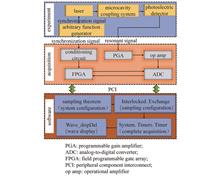
ObjectiveWhispering-gallery-mode optical micro-cavities have been extensively researched in narrow linewidth filters, biosensors, and nonlinear optics due to their small mode volume and ultra-high Q factor. Data acquisition and identification of mode spectral lines in real time are critical for experimental process control and index detection in research on optical micro-cavities. There are two typical detection strategies for spectral signals of optical micro-cavities. The first scheme uses a broadband light source to excite the whispering gallery modes of the optical micro-cavities, and the spectral signals are detected and evaluated by a spectrometer. It is costly, however, and thus this approach is only suitable for optical micro-cavities with a Q factor of less than 106. The other method for detecting spectral signals is to stimulate the whispering gallery modes by scanning the optical micro-cavity with a narrow linewidth laser. The stimulated spectral signal is then transformed by a photoelectric detector and sent to an oscilloscope for analysis. This approach is appropriate for ultra-high-Q optical micro-cavities, but it is incapable of analyzing the spectral signal in real time. In addition, there is an urgent need for an acquisition system with a high sampling rate, a rapid reaction time, and the capacity to monitor and analyze spectral data in real time for applications in high-sensitivity sensing of micro-cavities. Hence, a spectral signal acquisition system for optical micro-cavities is explored and constructed in this study to solve these issues. The system consists of an acquisition module, a data storage module, a data analysis module, and a data display module, which can show and analyze the spectral signals of optical micro-cavities in real time and has the benefit of quick acquisition. Moreover, it can set an arbitrary sampling interval and sampling time according to the requirements of different sensing systems, which solves the problems of capturing, analyzing, and displaying spectral signals in optical micro-cavities.MethodsThis signal acquisition system is separated into acquisition and software modules (Fig. 1). The analog signal is amplified and filtered by the conditioning circuit in the acquisition module (Fig. 2) before being transformed into a digital signal by the analog-to-digital converter (ADC). The transformed data stream is then transmitted to the processor for signal processing before the peripheral component interface (PCI) communicates with the upper computer software for data transmission, and the display operation is finished in the upper computer software. The acquisition system's software module is separated into five sections: trigger edge setting, system configuration, acquisition configuration, main menu, and data display. The trigger acquisition operation can be specified as a rising or trailing edge of the waveform in the trigger edge setting, and the rising edge trigger is valid at the positive edge. The time interval, sampling frequency, trigger frequency, and reference voltage can all be adjusted flexibly in the system configuration. After the parameters are set, they could be locked by the parameter lock feature in the system configuration to ensure the smooth execution of the acquisition procedure. The function of the acquisition configuration section is primarily to finish the setup of arbitrary parameters necessary for the number of acquisitions and the average number of acquisition experiments and control the acquisition process. The procedure of initiating and terminating the acquisition is completed via the main menu. The data display section shows the real-time waveform that is delivered to the upper computer software via NI Measurement Studio control. The development and design of the upper computer software for the acquisition system make use of Visual Studio software, which is equipped with the NI Measurement Studio integrated suite and is written in the C# programming language. The integrated suite provides a set of tightly integrated. NET controls for the Microsoft Visual Studio.NET environment, which allows the user to build virtual instrumentation systems.Results and DiscussionsFirst, the fundamental function of the spectral signal acquisition system is validated (Fig. 5), and the system's feasible basic acquisition function is proven. Then, the stability of the acquisition system is examined (Fig. 6), and the experimental findings reveal that the acquisition system fully fulfills the stability criteria of optical micro-acquisition cavities. After that, a fiber microsphere cavity created by arc discharge (Fig. 8) and a silica crystalline micro-disk cavity prepared by ultra-precision polishing (Fig. 9) are examined separately. The transmission spectra of the fiber microsphere cavity and the silica crystal micro-disk cavity are measured and traced, with the Q factor of the former being 2.26×10⁶ and that of the latter being 109. The acquisition system can excellently suppress noise and maintain steady mode spectral lines over extended periods. The optical micro-cavity system with an ultra-high Q factor has high reliability and could be utilized to create future micro-cavity sensing applications.ConclusionsA spectral signal acquisition system is designed for experimental systems of optical micro-cavities with an ultra-high Q factor. First, the triangle wave signal generated by the arbitrary function generator is acquired to evaluate the performance of this spectral acquisition system. It is demonstrated that this acquisition system can perform the fundamental acquisition function and has long-term stability. Second, this system is used to examine the spectral signal of a high-Q fiber microsphere cavity. The results indicate that this system is capable of realizing the flexible configuration of sampling of the micro-cavity system. Finally, the denoising feature of the ultra-high-Q silica crystal micro-disk cavity is shown by this system. The results show that the developed spectral signal acquisition system has the advantages of high reliability, a high sampling rate, and fast response, and it can acquire the spectral signals of ultra-high-Q micro-cavities and analyze the modes in real time. It provides great convenience for spectrum acquisition in micro-cavity research and can greatly broaden the potential applications of optical micro-cavity devices. ObjectiveWhispering-gallery-mode optical micro-cavities have been extensively researched in narrow linewidth filters, biosensors, and nonlinear optics due to their small mode volume and ultra-high Q factor. Data acquisition and identification of mode spectral lines in real time are critical for experimental process control and index detection in research on optical micro-cavities. There are two typical detection strategies for spectral signals of optical micro-cavities. The first scheme uses a broadband light source to excite the whispering gallery modes of the optical micro-cavities, and the spectral signals are detected and evaluated by a spectrometer. It is costly, however, and thus this approach is only suitable for optical micro-cavities with a Q factor of less than 106. The other method for detecting spectral signals is to stimulate the whispering gallery modes by scanning the optical micro-cavity with a narrow linewidth laser. The stimulated spectral signal is then transformed by a photoelectric detector and sent to an oscilloscope for analysis. This approach is appropriate for ultra-high-Q optical micro-cavities, but it is incapable of analyzing the spectral signal in real time. In addition, there is an urgent need for an acquisition system with a high sampling rate, a rapid reaction time, and the capacity to monitor and analyze spectral data in real time for applications in high-sensitivity sensing of micro-cavities. Hence, a spectral signal acquisition system for optical micro-cavities is explored and constructed in this study to solve these issues. The system consists of an acquisition module, a data storage module, a data analysis module, and a data display module, which can show and analyze the spectral signals of optical micro-cavities in real time and has the benefit of quick acquisition. Moreover, it can set an arbitrary sampling interval and sampling time according to the requirements of different sensing systems, which solves the problems of capturing, analyzing, and displaying spectral signals in optical micro-cavities.MethodsThis signal acquisition system is separated into acquisition and software modules (Fig. 1). The analog signal is amplified and filtered by the conditioning circuit in the acquisition module (Fig. 2) before being transformed into a digital signal by the analog-to-digital converter (ADC). The transformed data stream is then transmitted to the processor for signal processing before the peripheral component interface (PCI) communicates with the upper computer software for data transmission, and the display operation is finished in the upper computer software. The acquisition system's software module is separated into five sections: trigger edge setting, system configuration, acquisition configuration, main menu, and data display. The trigger acquisition operation can be specified as a rising or trailing edge of the waveform in the trigger edge setting, and the rising edge trigger is valid at the positive edge. The time interval, sampling frequency, trigger frequency, and reference voltage can all be adjusted flexibly in the system configuration. After the parameters are set, they could be locked by the parameter lock feature in the system configuration to ensure the smooth execution of the acquisition procedure. The function of the acquisition configuration section is primarily to finish the setup of arbitrary parameters necessary for the number of acquisitions and the average number of acquisition experiments and control the acquisition process. The procedure of initiating and terminating the acquisition is completed via the main menu. The data display section shows the real-time waveform that is delivered to the upper computer software via NI Measurement Studio control. The development and design of the upper computer software for the acquisition system make use of Visual Studio software, which is equipped with the NI Measurement Studio integrated suite and is written in the C# programming language. The integrated suite provides a set of tightly integrated. NET controls for the Microsoft Visual Studio.NET environment, which allows the user to build virtual instrumentation systems.Results and DiscussionsFirst, the fundamental function of the spectral signal acquisition system is validated (Fig. 5), and the system's feasible basic acquisition function is proven. Then, the stability of the acquisition system is examined (Fig. 6), and the experimental findings reveal that the acquisition system fully fulfills the stability criteria of optical micro-acquisition cavities. After that, a fiber microsphere cavity created by arc discharge (Fig. 8) and a silica crystalline micro-disk cavity prepared by ultra-precision polishing (Fig. 9) are examined separately. The transmission spectra of the fiber microsphere cavity and the silica crystal micro-disk cavity are measured and traced, with the Q factor of the former being 2.26×10⁶ and that of the latter being 109. The acquisition system can excellently suppress noise and maintain steady mode spectral lines over extended periods. The optical micro-cavity system with an ultra-high Q factor has high reliability and could be utilized to create future micro-cavity sensing applications.ConclusionsA spectral signal acquisition system is designed for experimental systems of optical micro-cavities with an ultra-high Q factor. First, the triangle wave signal generated by the arbitrary function generator is acquired to evaluate the performance of this spectral acquisition system. It is demonstrated that this acquisition system can perform the fundamental acquisition function and has long-term stability. Second, this system is used to examine the spectral signal of a high-Q fiber microsphere cavity. The results indicate that this system is capable of realizing the flexible configuration of sampling of the micro-cavity system. Finally, the denoising feature of the ultra-high-Q silica crystal micro-disk cavity is shown by this system. The results show that the developed spectral signal acquisition system has the advantages of high reliability, a high sampling rate, and fast response, and it can acquire the spectral signals of ultra-high-Q micro-cavities and analyze the modes in real time. It provides great convenience for spectrum acquisition in micro-cavity research and can greatly broaden the potential applications of optical micro-cavity devices.
Acta Optica Sinica
- Publication Date: Mar. 10, 2023
- Vol. 43, Issue 5, 0513001 (2023)

Silicon Mode Splitter Obtained by Inverse Design Based on Adjoint Method
Tao Chen, Siqiang Mao, Hongdan Wan, Jingli Wang, and Weifeng Jiang
ObjectiveSpace division multiplexing (SDM) technology has emerged to break through the transportation capacity limitations. As an important technical route to achieve SDM, mode division multiplexing (MDM) technology features high information density, low transmission cost, and low energy consumption. According to our investigation and research findings, there are many in-depth studies and reports on the implementation of various components in MDM systems. However, there is little research on the mode splitter. In MDM systems, mode-sensitive components have selectivity for input and output waveguide modes, and mode splitting based on a traditional mode demultiplexer is difficult to meet the requirements. Therefore, employing a mode splitter that does not change the mode order is an important method to improve the flexibility of MDM systems. The silicon-based mode splitter is a key device for constructing an on-chip MDM system to realize flexible routing of different modes. We propose a compact silicon-based mode splitter based on an adjoint optimization design algorithm and adopt the 3D full-vectorial finite-difference time domain (3D-FV-FDTD) for simulation verification. The simulated results show that the performance of the designed mode splitter meets the design targets, such as small size, low insertion loss and crosstalk, and large bandwidth. Thus the splitter can be applied to on-chip MDM systems, providing a viable device for high-capacity on-chip optical communications and optical interconnects.MethodsTraditional design depends on the researchers' experience to achieve design goals by optimizing structure parameters. By contrast, the inverse design method is a goal-oriented approach that utilizes inverse algorithms to design various structures, which could reduce design complexity and improve design efficiency. We leverage an inverse design method to optimize the structure. The whole design process is divided into five steps as shown in Fig. 3, including initializing structure parameters, simulating and calculating gradient, binarization, designing for manufacturing, and exporting files. Step 1 is determining the design target and initializing structure parameters. The designed mode splitter is composed of three rectangular waveguides and a functional region (Fig. 1). Step 2 is simulating and calculating gradients. The adjoint algorithm can calculate the derivatives of all points in the space and requires only two simulation processes in each iteration. The derivatives of all points could fine-tune the structure. Step 3 is forcing the material index to values at the upper and lower bounds to create a structure that can be defined by etching. Step 4 is designing for manufacturing. The minimum feature size in the design is constrained based on the target photolithography process. The final step is exporting the files, where the mode splitter based on inverse design can separate the TE0 mode and TE1 mode, and the characteristics such as crosstalk, insertion loss, and fabrication tolerance are analyzed by the 3D-FV-FDTD method.Results and DiscussionsSimulation results show that the optimized mode splitter can efficiently separate the TE0 mode and TE1 mode. When the TE0 mode is input, the insertion loss and crosstalk at the center wavelength are calculated to be 0.14 dB and -23.8 dB respectively, and when the TE1 mode is input, the insertion loss and crosstalk are 0.48 dB and -22.45 dB respectively (Fig. 6). The operating bandwidth covers 150 nm, and the insertion losses of TE0 and TE1 modes are lower than 0.44 dB and 1.16 dB, respectively. Additionally, we analyze 13 mode splitters with fabrication errors from -30 nm to 30 nm. At the center wavelength, when the TE0 mode is input, the insertion loss and crosstalk at the center wavelength are lower than 0.87 dB and -14.29 dB respectively, and when the TE1 mode is input, the insertion loss and crosstalk are lower than 1.59 dB and -10.45 dB respectively (Fig. 6). The ±15 nm fabrication tolerance is analyzed based on the 3D-FV-FDTD method. The insertion losses of the two modes are lower than 0.79 dB, with the crosstalk lower than -18.37 dB (Fig. 7).ConclusionsWe propose and optimally design an on-chip silicon mode splitter based on the inverse algorithm incorporating an adjoint algorithm. The high performances of insertion loss and mode crosstalk are achieved within the operating wavelength from 1500 nm to 1650 nm. The optimized mode splitter can be obtained within 148 iterations, in which each iteration only requires two FDTD simulation steps. The simulation results show that at the center wavelength, the insertion loss and mode crosstalk of the TE0 mode are less than 0.14 dB and -23.8 dB respectively, and those of the TE1 mode are less than 0.48 dB and -22.45 dB respectively. The fabrication tolerances of the optimized mode splitter are also investigated with the fabrication errors of ±30 nm. A competitive performance can also be kept with an overall error of ±15 nm. A compact footprint of only 5.5 μm×4 μm and a wide operating bandwidth are realized. Our mode splitter could be applied to on-chip MDM systems, providing a viable device for high-capacity on-chip optical communications and optical interconnects. ObjectiveSpace division multiplexing (SDM) technology has emerged to break through the transportation capacity limitations. As an important technical route to achieve SDM, mode division multiplexing (MDM) technology features high information density, low transmission cost, and low energy consumption. According to our investigation and research findings, there are many in-depth studies and reports on the implementation of various components in MDM systems. However, there is little research on the mode splitter. In MDM systems, mode-sensitive components have selectivity for input and output waveguide modes, and mode splitting based on a traditional mode demultiplexer is difficult to meet the requirements. Therefore, employing a mode splitter that does not change the mode order is an important method to improve the flexibility of MDM systems. The silicon-based mode splitter is a key device for constructing an on-chip MDM system to realize flexible routing of different modes. We propose a compact silicon-based mode splitter based on an adjoint optimization design algorithm and adopt the 3D full-vectorial finite-difference time domain (3D-FV-FDTD) for simulation verification. The simulated results show that the performance of the designed mode splitter meets the design targets, such as small size, low insertion loss and crosstalk, and large bandwidth. Thus the splitter can be applied to on-chip MDM systems, providing a viable device for high-capacity on-chip optical communications and optical interconnects.MethodsTraditional design depends on the researchers' experience to achieve design goals by optimizing structure parameters. By contrast, the inverse design method is a goal-oriented approach that utilizes inverse algorithms to design various structures, which could reduce design complexity and improve design efficiency. We leverage an inverse design method to optimize the structure. The whole design process is divided into five steps as shown in Fig. 3, including initializing structure parameters, simulating and calculating gradient, binarization, designing for manufacturing, and exporting files. Step 1 is determining the design target and initializing structure parameters. The designed mode splitter is composed of three rectangular waveguides and a functional region (Fig. 1). Step 2 is simulating and calculating gradients. The adjoint algorithm can calculate the derivatives of all points in the space and requires only two simulation processes in each iteration. The derivatives of all points could fine-tune the structure. Step 3 is forcing the material index to values at the upper and lower bounds to create a structure that can be defined by etching. Step 4 is designing for manufacturing. The minimum feature size in the design is constrained based on the target photolithography process. The final step is exporting the files, where the mode splitter based on inverse design can separate the TE0 mode and TE1 mode, and the characteristics such as crosstalk, insertion loss, and fabrication tolerance are analyzed by the 3D-FV-FDTD method.Results and DiscussionsSimulation results show that the optimized mode splitter can efficiently separate the TE0 mode and TE1 mode. When the TE0 mode is input, the insertion loss and crosstalk at the center wavelength are calculated to be 0.14 dB and -23.8 dB respectively, and when the TE1 mode is input, the insertion loss and crosstalk are 0.48 dB and -22.45 dB respectively (Fig. 6). The operating bandwidth covers 150 nm, and the insertion losses of TE0 and TE1 modes are lower than 0.44 dB and 1.16 dB, respectively. Additionally, we analyze 13 mode splitters with fabrication errors from -30 nm to 30 nm. At the center wavelength, when the TE0 mode is input, the insertion loss and crosstalk at the center wavelength are lower than 0.87 dB and -14.29 dB respectively, and when the TE1 mode is input, the insertion loss and crosstalk are lower than 1.59 dB and -10.45 dB respectively (Fig. 6). The ±15 nm fabrication tolerance is analyzed based on the 3D-FV-FDTD method. The insertion losses of the two modes are lower than 0.79 dB, with the crosstalk lower than -18.37 dB (Fig. 7).ConclusionsWe propose and optimally design an on-chip silicon mode splitter based on the inverse algorithm incorporating an adjoint algorithm. The high performances of insertion loss and mode crosstalk are achieved within the operating wavelength from 1500 nm to 1650 nm. The optimized mode splitter can be obtained within 148 iterations, in which each iteration only requires two FDTD simulation steps. The simulation results show that at the center wavelength, the insertion loss and mode crosstalk of the TE0 mode are less than 0.14 dB and -23.8 dB respectively, and those of the TE1 mode are less than 0.48 dB and -22.45 dB respectively. The fabrication tolerances of the optimized mode splitter are also investigated with the fabrication errors of ±30 nm. A competitive performance can also be kept with an overall error of ±15 nm. A compact footprint of only 5.5 μm×4 μm and a wide operating bandwidth are realized. Our mode splitter could be applied to on-chip MDM systems, providing a viable device for high-capacity on-chip optical communications and optical interconnects.
Acta Optica Sinica
- Publication Date: Dec. 10, 2023
- Vol. 43, Issue 23, 2313003 (2023)
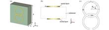
Theoretical Analysis and Experimental Investigation of Silicon-Organic Hybrid Integrated Electro-Optic Modulator with Traveling-Wave Electrodes
Zihan Zhou, Meng Chao, Xinxin Su, Zhuo Chen, Ruonan Liu, Shuhui Bo, Zhihua Li, Zhenlin Wu, Mingshan Zhao, and Xiuyou Han
ObjectiveWith the rapid development of communication technology, the coverage area, transmission bandwidth, energy efficiency ratio, and device size of communication networks have higher requirements. Optical communication network using lightwave as the information carrier has become a very competitive technology development direction due to its characteristics of ultra-wide bandwidth, low delay, and low loss. Electro-optic modulator (EOM) is one of the most important optoelectronic devices in optical communication systems and microwave photonic systems, and its characteristics directly affect the performance of optoelectronic information systems. The function of the EOM is to convert the signal from the electrical domain to the optical domain and then to process and transmit the signal. After a period of rapid development of optoelectronic technology, the entire system has gradually developed from discrete optical devices to board-level interconnection and on-chip integration, especially the array and multifunctional integration needs of optoelectronic information systems make highly integrated optoelectronic chips an inevitable trend of technological development. In order to meet the application requirements of a larger range, higher speed, and higher energy efficiency of photoelectric information processing, the development of integrated electro-optic modulators with larger bandwidth, lower half-wave voltage, and smaller volume is one of the important directions of photoelectric integration technology.MethodsThe silicon-organic hybrid (SOH) integrated EOM with traveling-wave electrode structure is investigated. The mathematical model of an EOM with the traveling-wave electrode is established, and the effects of the group refractive index of lightwave, effective refractive index of microwave, and characteristic impedance of the modulator on the electro-optic modulation response bandwidth are analyzed. Under the guidance of the theoretical model, the traveling-wave electrode structure of the SOH-integrated EOM is optimized, and the fabrication of the silicon optical waveguide device and the on-chip polarization of the electro-optical polymer are completed by the domestic process platform.Results and DiscussionsAccording to the theoretical model, the corresponding electro-optical bandwidths under different impedance matching and velocity matching conditions are simulated, and the matching state under the maximum bandwidth condition is that the speed between the lightwave and the microwave is perfectly matched, and the characteristic impedance of the modulator is slightly greater than the system impedance (50 Ω), as shown in Fig. 6 and Fig. 7. The electrode structure of the modulator is simulated and optimized, and the electrical bandwidth is greater than 80 GHz. The effective refractive index of a microwave is about 3.3, and the characteristic impedance is about 37 Ω. The fabrication and on-chip polarization of the modulator chip are completed (Figs. 10-12), and the electrical tests of the modulator are carried out. The measured electrical bandwidth of the modulator is greater than 60 GHz, and the characteristic impedance of the electrode is calculated to be about 45 Ω, with an effective refractive index of 4.5 (Fig. 13 and Fig. 14). The final modulation effect of the modulator is tested, and the electro-optic modulation bandwidth greater than 50 GHz is obtained (Fig. 16).ConclusionsIn this paper, the traveling-wave electrode structure model of SOH-integrated EOM is established, and its working principle is theoretically deduced in detail. The effects of electrode characteristic impedance and microwave effective refractive index on the response bandwidth of electro-optic modulation are analyzed. On this basis, an SOH integrated EOM is designed and fabricated, and the high-performance electro-optic modulation is obtained by exploring the on-chip polarization process of electro-optical polymer material. The experimental system is set up to test and analyze the characteristics of the modulator chip, and the 3 dB electro-optic modulation response bandwidth of 50 GHz is measured. The experimental results are in good agreement with the theoretical calculation results, which verifies the validity of the structure model of the traveling-wave electrode. The theoretical modeling analysis and experimental research work in this paper provide a good foundation for further improving the performance of SOH-integrated EOMs. ObjectiveWith the rapid development of communication technology, the coverage area, transmission bandwidth, energy efficiency ratio, and device size of communication networks have higher requirements. Optical communication network using lightwave as the information carrier has become a very competitive technology development direction due to its characteristics of ultra-wide bandwidth, low delay, and low loss. Electro-optic modulator (EOM) is one of the most important optoelectronic devices in optical communication systems and microwave photonic systems, and its characteristics directly affect the performance of optoelectronic information systems. The function of the EOM is to convert the signal from the electrical domain to the optical domain and then to process and transmit the signal. After a period of rapid development of optoelectronic technology, the entire system has gradually developed from discrete optical devices to board-level interconnection and on-chip integration, especially the array and multifunctional integration needs of optoelectronic information systems make highly integrated optoelectronic chips an inevitable trend of technological development. In order to meet the application requirements of a larger range, higher speed, and higher energy efficiency of photoelectric information processing, the development of integrated electro-optic modulators with larger bandwidth, lower half-wave voltage, and smaller volume is one of the important directions of photoelectric integration technology.MethodsThe silicon-organic hybrid (SOH) integrated EOM with traveling-wave electrode structure is investigated. The mathematical model of an EOM with the traveling-wave electrode is established, and the effects of the group refractive index of lightwave, effective refractive index of microwave, and characteristic impedance of the modulator on the electro-optic modulation response bandwidth are analyzed. Under the guidance of the theoretical model, the traveling-wave electrode structure of the SOH-integrated EOM is optimized, and the fabrication of the silicon optical waveguide device and the on-chip polarization of the electro-optical polymer are completed by the domestic process platform.Results and DiscussionsAccording to the theoretical model, the corresponding electro-optical bandwidths under different impedance matching and velocity matching conditions are simulated, and the matching state under the maximum bandwidth condition is that the speed between the lightwave and the microwave is perfectly matched, and the characteristic impedance of the modulator is slightly greater than the system impedance (50 Ω), as shown in Fig. 6 and Fig. 7. The electrode structure of the modulator is simulated and optimized, and the electrical bandwidth is greater than 80 GHz. The effective refractive index of a microwave is about 3.3, and the characteristic impedance is about 37 Ω. The fabrication and on-chip polarization of the modulator chip are completed (Figs. 10-12), and the electrical tests of the modulator are carried out. The measured electrical bandwidth of the modulator is greater than 60 GHz, and the characteristic impedance of the electrode is calculated to be about 45 Ω, with an effective refractive index of 4.5 (Fig. 13 and Fig. 14). The final modulation effect of the modulator is tested, and the electro-optic modulation bandwidth greater than 50 GHz is obtained (Fig. 16).ConclusionsIn this paper, the traveling-wave electrode structure model of SOH-integrated EOM is established, and its working principle is theoretically deduced in detail. The effects of electrode characteristic impedance and microwave effective refractive index on the response bandwidth of electro-optic modulation are analyzed. On this basis, an SOH integrated EOM is designed and fabricated, and the high-performance electro-optic modulation is obtained by exploring the on-chip polarization process of electro-optical polymer material. The experimental system is set up to test and analyze the characteristics of the modulator chip, and the 3 dB electro-optic modulation response bandwidth of 50 GHz is measured. The experimental results are in good agreement with the theoretical calculation results, which verifies the validity of the structure model of the traveling-wave electrode. The theoretical modeling analysis and experimental research work in this paper provide a good foundation for further improving the performance of SOH-integrated EOMs.
Acta Optica Sinica
- Publication Date: Dec. 10, 2023
- Vol. 43, Issue 23, 2313002 (2023)
Design and Verification of Single-Photon Avalanche Diode with High Gain at Low Overbias Voltage
Rongqing Yi, Yang Wang, Zhixiang Cao, and Xiangliang Jin
ObjectivePhotoelectric detection plays an important role in various fields such as fluorescence microscopes, photodetectors, and medical three-dimensional imaging. With the emergence of photomultiplier tubes (PMTs), avalanche photodiodes (APDs), and other new photoelectric devices, the photoelectric detection effect is further strengthened. PMT achieves high sensitivity detection by photoelectron multiplication, but it features expensiveness, fragility, large size, and high pressure operation, which makes it have limited practical applications. Meanwhile, APDs based on the avalanche effect can generate avalanche current amplification under light excitation, but it is limited by gain, volume, process compatibility, and other factors in practical applications. Single-photon avalanche diode (SPAD) has been applied to various fields such as robotic radar detection, target tracking, and autonomous driving due to its low power consumption, high sensitivity, and low noise characteristics. Most of the SPADs proposed in recent years have high photon detection probability (PDP) under high overbias voltage or enlarge the multiplication region to achieve higher detection probability, but this will affect the junction capacitance and then the time jitter of the device. Thus, we design a SPAD device compatible with most of the processes, which can achieve high PDP at low overbias voltage and has a small dark count rate (DCR).MethodsThe basic working mechanism of SPAD is characterized by applying technology-computer-aided-design (TCAD) software. Silvaco TCAD software is employed to simulate the device structure and obtain electrical characteristic results from the Atlas Simulator. The Selberrherr model (impact ionization model) built into TCAD software is adopted for analyzing the operating mechanism, and the Newton iteration method is for numerical calculation. Then, a SPAD device with N+/P-well is designed based on a 180 nm standard bipolar CMOS-DMOS (BCD) process, and the device performance is tested by qE-IPCE-K6517B UV detector photoelectric response system and semiconductor analyzer. Additionally, based on the Cadence circuit simulation platform, VerilogA programming language and circuit combined hybrid model are built to simulate SPAD quenching and I-V curve, which provides guidance for SPAD design in the future.Results and DiscussionsSimulation results show that the N+/P-well structure has a large electric field and current density in the avalanche multiplication region. The breakdown voltage of the device is about 12.8 V, and photo-generated carriers in the depletion region collide with lattice atoms to create new electron-hole pairs. This chain reaction makes the number of charge carriers in the depletion layer increase in an avalanche manner, and the current flowing through the PN junction rises sharply. Breakdown voltage testing of the flow sheet device indicates that the photocurrent in the linear region of the SPAD can reach the sub-microamperage level. The test results show that the device's PDP can reach 42.7% under the overbias voltage of 1 V, peak wavelength is 560 nm, and DCR is 11.5 Hz/μm2. The built model is verified to be consistent with the measured principle of the device, and an avalanche pulse can be generated when a photon arrives and is passively quenched by a quench resistor. The matching results of light and dark currents can well fit the measured I-V characteristics of SPAD.ConclusionsA SPAD device with high PDP is designed based on a 180 nm standard BCD process. The device has good spectral responses in the range of 440-740 nm. An N+/P-well with a radius of 10 μm is adopted to form a PN junction as the sensing region, and a protective ring that effectively prevents edge breakdown is formed by the N-well. The basic working mechanism of SPAD is characterized by applying TCAD software. The actual electrical parameters of the device are also obtained by the established test platform. The test results show that more than 30% PDP can be achieved in the wavelength range of 480-660 nm at an overbias voltage of 1 V. At 560 nm, the peak PDP is 42.7% and the DCR is 11.5 Hz/μm2. Finally, the VerilogA hybrid model verifies the good agreement between the simulated and measured results. ObjectivePhotoelectric detection plays an important role in various fields such as fluorescence microscopes, photodetectors, and medical three-dimensional imaging. With the emergence of photomultiplier tubes (PMTs), avalanche photodiodes (APDs), and other new photoelectric devices, the photoelectric detection effect is further strengthened. PMT achieves high sensitivity detection by photoelectron multiplication, but it features expensiveness, fragility, large size, and high pressure operation, which makes it have limited practical applications. Meanwhile, APDs based on the avalanche effect can generate avalanche current amplification under light excitation, but it is limited by gain, volume, process compatibility, and other factors in practical applications. Single-photon avalanche diode (SPAD) has been applied to various fields such as robotic radar detection, target tracking, and autonomous driving due to its low power consumption, high sensitivity, and low noise characteristics. Most of the SPADs proposed in recent years have high photon detection probability (PDP) under high overbias voltage or enlarge the multiplication region to achieve higher detection probability, but this will affect the junction capacitance and then the time jitter of the device. Thus, we design a SPAD device compatible with most of the processes, which can achieve high PDP at low overbias voltage and has a small dark count rate (DCR).MethodsThe basic working mechanism of SPAD is characterized by applying technology-computer-aided-design (TCAD) software. Silvaco TCAD software is employed to simulate the device structure and obtain electrical characteristic results from the Atlas Simulator. The Selberrherr model (impact ionization model) built into TCAD software is adopted for analyzing the operating mechanism, and the Newton iteration method is for numerical calculation. Then, a SPAD device with N+/P-well is designed based on a 180 nm standard bipolar CMOS-DMOS (BCD) process, and the device performance is tested by qE-IPCE-K6517B UV detector photoelectric response system and semiconductor analyzer. Additionally, based on the Cadence circuit simulation platform, VerilogA programming language and circuit combined hybrid model are built to simulate SPAD quenching and I-V curve, which provides guidance for SPAD design in the future.Results and DiscussionsSimulation results show that the N+/P-well structure has a large electric field and current density in the avalanche multiplication region. The breakdown voltage of the device is about 12.8 V, and photo-generated carriers in the depletion region collide with lattice atoms to create new electron-hole pairs. This chain reaction makes the number of charge carriers in the depletion layer increase in an avalanche manner, and the current flowing through the PN junction rises sharply. Breakdown voltage testing of the flow sheet device indicates that the photocurrent in the linear region of the SPAD can reach the sub-microamperage level. The test results show that the device's PDP can reach 42.7% under the overbias voltage of 1 V, peak wavelength is 560 nm, and DCR is 11.5 Hz/μm2. The built model is verified to be consistent with the measured principle of the device, and an avalanche pulse can be generated when a photon arrives and is passively quenched by a quench resistor. The matching results of light and dark currents can well fit the measured I-V characteristics of SPAD.ConclusionsA SPAD device with high PDP is designed based on a 180 nm standard BCD process. The device has good spectral responses in the range of 440-740 nm. An N+/P-well with a radius of 10 μm is adopted to form a PN junction as the sensing region, and a protective ring that effectively prevents edge breakdown is formed by the N-well. The basic working mechanism of SPAD is characterized by applying TCAD software. The actual electrical parameters of the device are also obtained by the established test platform. The test results show that more than 30% PDP can be achieved in the wavelength range of 480-660 nm at an overbias voltage of 1 V. At 560 nm, the peak PDP is 42.7% and the DCR is 11.5 Hz/μm2. Finally, the VerilogA hybrid model verifies the good agreement between the simulated and measured results.
Acta Optica Sinica
- Publication Date: Dec. 10, 2023
- Vol. 43, Issue 23, 2313001 (2023)
Multipole Method Analysis of Waveguides Based on Graphene-Coated Double Elliptical and Cylindrical Parallel Nanowires
Yida Du, Ning Li, Wenrui Xue, Huihui Li, Yue Zhang, and Changyong Li
ObjectiveThe waveguide structure based on graphene materials has been a research hotspot in recent years. By employing the finite element method (FEM), the characteristics of the five lowest-order modes supported by the waveguide based on graphene-coated double elliptical and cylindrical parallel nanowires were reported. Since a purely numerical method is adopted in this study, it is impossible to give a clear physical image of the mode formation mechanism. To this end, we intend to employ the multipole method (MPM) to reanalyze the fundamental mode of the waveguide structure discussed before, and give a clear physical image of the mode formation mechanism. Meanwhile, the MPM correctness is verified by comparing the relative error between the results of the two calculation methods with the maximum value of the term number expanded by the MPM, the working wavelength, the Fermi energy, the semi-major and semi-minor axes of the elliptical cylindrical nanowires, the lateral spacing between the surfaces of the nanowires, and the relative height of the cylindrical nanowires.MethodsWe leverage the MPM to calculate the characteristics of modes supported by the waveguide based on graphene-coated double elliptical and cylindrical parallel nanowires. First, we assume that the double elliptical cylindrical nanowires and the cylindrical nanowire exist alone and that the longitudinal components of the field are expanded into series form in their coordinate systems respectively. Then, according to the field superposition principle, the longitudinal components of the field in each region of the combined waveguide are obtained. Then, the radial and angular components of the field are obtained by the relationship between the lateral component and the longitudinal component of the field. The involved derivatives can be obtained via the gradient of the scalar field and the point product of the unit vector. Then, graphene is regarded as a conductor boundary without thickness, and a linear algebraic equation system is established by the boundary relationship and point-by-point matching method. Finally, the effective refractive index and field distribution of modes supported by the waveguide can be obtained by solving this system of linear algebraic equations.Results and DiscussionsAny change in the number of series expansion terms, the operating wavelength, the Fermi energy, and the structure parameters of the waveguide will affect the MPM accuracy. The relative errors of the real and imaginary parts of the effective refractive index calculated by the MPM and the FEM decrease as the Mmax values increase (Fig. 3). As the working wavelength increases from 8.0 to 10.0 μm and Fermi energy increases from 0.35 to 0.60 eV, the relative error rises (Figs. 4 and 5). When the radius of the cylindrical dielectric nanowire increases from 42 to 58 nm, the semi-major axis of the elliptic cylindrical nanowire grows from 96 to 104 nm, with the increased relative error of the real part of the effective refractive index and decreased relative error of the imaginary part of the effective refractive index (Figs. 6 and 7). When the short half axis of the elliptic cylindrical nanowire increases from 91 to 99 nm, the relative error of the real part of the effective refractive index reduces and the imaginary part of the effective refractive index rises (Fig. 8). As the transverse spacing between the nanowire surfaces increases from 12 to 28 nm, and the relative height of the cylindrical nanowire rises from 50 to 66 nm, the relative error of the effective refractive index decreases (Figs. 9 and 10). These phenomena can be explained by the field distribution in space. Since the MPM ignores the nonlinear superposition effect of the field, the relative error increases under stronger coupling between the fields on the nanowire surface.ConclusionsThe results show that the larger number of series expansion terms leads to closer results of the MPM to those of the FEM, and the increasing working wavelength and Fermi energy bring about rising relative errors of the real and imaginary parts of the effective refractive index. As the radius of cylindrical dielectric nanowires and the major and semi-axial axes of elliptical cylindrical nanowires increase, the relative error of the real part of the effective refractive index rises, and that of the imaginary part of the effective refractive index decreases. Under the increasing short semi-axis of elliptical cylindrical nanowires, the relative error of the real part of the effective refractive index decreases, and that of the imaginary part of the effective refractive index rises. When the lateral spacing between the nanowire surfaces and the relative height of the cylindrical nanowires increases, the relative errors of the real and imaginary parts of the effective refractive index decrease. These phenomena can be explained by the field distribution. Within our calculation range, the relative errors are maintained on the order of 10-3. ObjectiveThe waveguide structure based on graphene materials has been a research hotspot in recent years. By employing the finite element method (FEM), the characteristics of the five lowest-order modes supported by the waveguide based on graphene-coated double elliptical and cylindrical parallel nanowires were reported. Since a purely numerical method is adopted in this study, it is impossible to give a clear physical image of the mode formation mechanism. To this end, we intend to employ the multipole method (MPM) to reanalyze the fundamental mode of the waveguide structure discussed before, and give a clear physical image of the mode formation mechanism. Meanwhile, the MPM correctness is verified by comparing the relative error between the results of the two calculation methods with the maximum value of the term number expanded by the MPM, the working wavelength, the Fermi energy, the semi-major and semi-minor axes of the elliptical cylindrical nanowires, the lateral spacing between the surfaces of the nanowires, and the relative height of the cylindrical nanowires.MethodsWe leverage the MPM to calculate the characteristics of modes supported by the waveguide based on graphene-coated double elliptical and cylindrical parallel nanowires. First, we assume that the double elliptical cylindrical nanowires and the cylindrical nanowire exist alone and that the longitudinal components of the field are expanded into series form in their coordinate systems respectively. Then, according to the field superposition principle, the longitudinal components of the field in each region of the combined waveguide are obtained. Then, the radial and angular components of the field are obtained by the relationship between the lateral component and the longitudinal component of the field. The involved derivatives can be obtained via the gradient of the scalar field and the point product of the unit vector. Then, graphene is regarded as a conductor boundary without thickness, and a linear algebraic equation system is established by the boundary relationship and point-by-point matching method. Finally, the effective refractive index and field distribution of modes supported by the waveguide can be obtained by solving this system of linear algebraic equations.Results and DiscussionsAny change in the number of series expansion terms, the operating wavelength, the Fermi energy, and the structure parameters of the waveguide will affect the MPM accuracy. The relative errors of the real and imaginary parts of the effective refractive index calculated by the MPM and the FEM decrease as the Mmax values increase (Fig. 3). As the working wavelength increases from 8.0 to 10.0 μm and Fermi energy increases from 0.35 to 0.60 eV, the relative error rises (Figs. 4 and 5). When the radius of the cylindrical dielectric nanowire increases from 42 to 58 nm, the semi-major axis of the elliptic cylindrical nanowire grows from 96 to 104 nm, with the increased relative error of the real part of the effective refractive index and decreased relative error of the imaginary part of the effective refractive index (Figs. 6 and 7). When the short half axis of the elliptic cylindrical nanowire increases from 91 to 99 nm, the relative error of the real part of the effective refractive index reduces and the imaginary part of the effective refractive index rises (Fig. 8). As the transverse spacing between the nanowire surfaces increases from 12 to 28 nm, and the relative height of the cylindrical nanowire rises from 50 to 66 nm, the relative error of the effective refractive index decreases (Figs. 9 and 10). These phenomena can be explained by the field distribution in space. Since the MPM ignores the nonlinear superposition effect of the field, the relative error increases under stronger coupling between the fields on the nanowire surface.ConclusionsThe results show that the larger number of series expansion terms leads to closer results of the MPM to those of the FEM, and the increasing working wavelength and Fermi energy bring about rising relative errors of the real and imaginary parts of the effective refractive index. As the radius of cylindrical dielectric nanowires and the major and semi-axial axes of elliptical cylindrical nanowires increase, the relative error of the real part of the effective refractive index rises, and that of the imaginary part of the effective refractive index decreases. Under the increasing short semi-axis of elliptical cylindrical nanowires, the relative error of the real part of the effective refractive index decreases, and that of the imaginary part of the effective refractive index rises. When the lateral spacing between the nanowire surfaces and the relative height of the cylindrical nanowires increases, the relative errors of the real and imaginary parts of the effective refractive index decrease. These phenomena can be explained by the field distribution. Within our calculation range, the relative errors are maintained on the order of 10-3.
Acta Optica Sinica
- Publication Date: Nov. 25, 2023
- Vol. 43, Issue 22, 2213002 (2023)
Bandwidth Compression of Microwave Photonic Filter Based on Cascaded Micro Rings
Pengfei Wang, Wei Cheng, Zhao Cang, Zhuang Tian, Zien Liang, Chen Guo, Yuhang Liu, and Binfeng Yun
ObjectiveMicrowave photonic technology can process radio frequency (RF) signals in the optical domain. Compared with the traditional electrical processing methods, it has the advantages of low loss, broadband, good tunability, and sound anti-electromagnetic interference. As an important component for various applications such as radar, communications, and radio astronomy, microwave photonic filter (MPF) has become a research hotspot in microwave photonics in recent years. With the development of photonic integration technology, integrated MPFs have attracted research attention. Recently, microring resonators (MRRs) have been widely employed in MPFs thanks to their compact sizes and good adjustability. The MPF should have a narrow RF bandwidth to achieve precise RF resolution. As known, typically the RF bandwidth of the MPF based on MRR is the same as the optical bandwidth of the MRR when crosstalk is ignored. Therefore, reducing the optical bandwidth of the MRR by improving its quality factor (Q factor) is the most direct and effective way to reduce the MPF bandwidth. However, the MRR loss should be reduced to increase the Q factor, which is difficult to achieve since the scattering loss caused by the waveguide sidewall roughness is usually unavoidable. Under typical silicon-on-insulator (SOI) fabrication processes, optical bandwidth of about GHz for MRR can be obtained, which cannot meet the requirements of high-precision MPF with sub-GHz frequency resolving capability. We propose and demonstrate an MPF based on three cascaded MRRs and phase modulation. With this configuration, the 3-dB RF bandwidth of the MPF can be well compressed compared with the 3-dB optical bandwidth of the MRR, and flexible tunability of the MPF is achieved.MethodsWe put forward an MPF based on cascaded three MRRs and phase modulation. By introducing two more MRRs, the phase differences between the optical carrier and the ±1 order optical sidebands can be changed much steeper from 0-π compared with the MPF constructed by a single MRR. As a result, the photocurrent obtained by beating the optical carrier and the ±1 order optical sidebands changes abruptly from constructive interference to destructive interference. Thus the slopes on both sides of the filter peak of the MPF response can be increased to achieve RF bandwidth compressing compared with that of the MPF based on a single MRR. Simulation and experimental results show that the MPF based on cascaded three MRRs and phase modulation can compress the RF bandwidth.Results and DiscussionsWe simulate the phase spectra of the optical carrier and the ±1 order optical sidebands of the MPF based on cascaded three MRRs and the MPF based on single MRR. The results show that the phase difference between 8.9-9.5 GHz for the MPF based on cascaded three MRRs is 1.12π, while the phase difference for the MPF based on single MRR is only 0.83π, which means much steeper phase changing from 0-π is achieved by the MPF based on three MRRs compared with the MPF based on single MRR [Fig. 4(b)]. Additionally, the simulation results show that compared with the MPF based on single MRR, the RF bandwidth of the MPF based on cascaded three MRRs is compressed by about 52%, and the 3-dB attenuation slope is increased about 1.1 times than that of the MPF based on single MRR [Fig. 4(d)] without enhancing the Q factor . The experimental results show that the MPF based on cascaded three MRRs can compress the RF bandwidth by about 69%, and the 3-dB attenuation slope is increased about 3.6 times than that of the MPF based on single MRR (Fig. 9). Meanwhile, continuous frequency tuning in the range of 11.5-20.3 GHz [Fig. 10(b)] and RF bandwidth tuning in the range of 187.1-1597.0 MHz [Fig. 10(a)] are achieved.ConclusionsWe propose and demonstrate a bandwidth compressing method for the MPF based on cascaded three MRRs and phase modulation. By adopting this method, the phase differences between the optical carrier and the ±1 order optical sidebands can be changed much steeper from 0-π than that of the MPF based on single MRR to compress the RF bandwidth of the MPF. Compared with the MPF based on single MRR, the RF bandwidth of the MPF based on cascaded three MRRs is compressed by about 69% without increasing the Q factor. Additionally, the 3-dB attenuation slope is increased about 3.6 times than that of the MPF based on single MRR. Continuous frequency tuning in the range of 11.5-20.3 GHz and RF bandwidth tuning in the range of 187.1-1597.0 MHz are achieved. Furthermore, the proposed method can achieve an even narrower RF bandwidth if an MRR with a higher Q factor is adopted. Meanwhile, the proposed MPF has the potential to be fully integrated into a chip and could find extensive utilization in microwave photonic signal processing systems. ObjectiveMicrowave photonic technology can process radio frequency (RF) signals in the optical domain. Compared with the traditional electrical processing methods, it has the advantages of low loss, broadband, good tunability, and sound anti-electromagnetic interference. As an important component for various applications such as radar, communications, and radio astronomy, microwave photonic filter (MPF) has become a research hotspot in microwave photonics in recent years. With the development of photonic integration technology, integrated MPFs have attracted research attention. Recently, microring resonators (MRRs) have been widely employed in MPFs thanks to their compact sizes and good adjustability. The MPF should have a narrow RF bandwidth to achieve precise RF resolution. As known, typically the RF bandwidth of the MPF based on MRR is the same as the optical bandwidth of the MRR when crosstalk is ignored. Therefore, reducing the optical bandwidth of the MRR by improving its quality factor (Q factor) is the most direct and effective way to reduce the MPF bandwidth. However, the MRR loss should be reduced to increase the Q factor, which is difficult to achieve since the scattering loss caused by the waveguide sidewall roughness is usually unavoidable. Under typical silicon-on-insulator (SOI) fabrication processes, optical bandwidth of about GHz for MRR can be obtained, which cannot meet the requirements of high-precision MPF with sub-GHz frequency resolving capability. We propose and demonstrate an MPF based on three cascaded MRRs and phase modulation. With this configuration, the 3-dB RF bandwidth of the MPF can be well compressed compared with the 3-dB optical bandwidth of the MRR, and flexible tunability of the MPF is achieved.MethodsWe put forward an MPF based on cascaded three MRRs and phase modulation. By introducing two more MRRs, the phase differences between the optical carrier and the ±1 order optical sidebands can be changed much steeper from 0-π compared with the MPF constructed by a single MRR. As a result, the photocurrent obtained by beating the optical carrier and the ±1 order optical sidebands changes abruptly from constructive interference to destructive interference. Thus the slopes on both sides of the filter peak of the MPF response can be increased to achieve RF bandwidth compressing compared with that of the MPF based on a single MRR. Simulation and experimental results show that the MPF based on cascaded three MRRs and phase modulation can compress the RF bandwidth.Results and DiscussionsWe simulate the phase spectra of the optical carrier and the ±1 order optical sidebands of the MPF based on cascaded three MRRs and the MPF based on single MRR. The results show that the phase difference between 8.9-9.5 GHz for the MPF based on cascaded three MRRs is 1.12π, while the phase difference for the MPF based on single MRR is only 0.83π, which means much steeper phase changing from 0-π is achieved by the MPF based on three MRRs compared with the MPF based on single MRR [Fig. 4(b)]. Additionally, the simulation results show that compared with the MPF based on single MRR, the RF bandwidth of the MPF based on cascaded three MRRs is compressed by about 52%, and the 3-dB attenuation slope is increased about 1.1 times than that of the MPF based on single MRR [Fig. 4(d)] without enhancing the Q factor . The experimental results show that the MPF based on cascaded three MRRs can compress the RF bandwidth by about 69%, and the 3-dB attenuation slope is increased about 3.6 times than that of the MPF based on single MRR (Fig. 9). Meanwhile, continuous frequency tuning in the range of 11.5-20.3 GHz [Fig. 10(b)] and RF bandwidth tuning in the range of 187.1-1597.0 MHz [Fig. 10(a)] are achieved.ConclusionsWe propose and demonstrate a bandwidth compressing method for the MPF based on cascaded three MRRs and phase modulation. By adopting this method, the phase differences between the optical carrier and the ±1 order optical sidebands can be changed much steeper from 0-π than that of the MPF based on single MRR to compress the RF bandwidth of the MPF. Compared with the MPF based on single MRR, the RF bandwidth of the MPF based on cascaded three MRRs is compressed by about 69% without increasing the Q factor. Additionally, the 3-dB attenuation slope is increased about 3.6 times than that of the MPF based on single MRR. Continuous frequency tuning in the range of 11.5-20.3 GHz and RF bandwidth tuning in the range of 187.1-1597.0 MHz are achieved. Furthermore, the proposed method can achieve an even narrower RF bandwidth if an MRR with a higher Q factor is adopted. Meanwhile, the proposed MPF has the potential to be fully integrated into a chip and could find extensive utilization in microwave photonic signal processing systems.
Acta Optica Sinica
- Publication Date: Nov. 25, 2023
- Vol. 43, Issue 22, 2213001 (2023)
Topics
© Copyright 2018-2021 | Chinese Laser Press. All Rights Reserved 沪ICP备15018463号-20